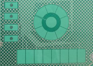
Designing Capacitive Touch Keypad
Capacitive touch keypad uses the same materials as the standard resistive membrane switch, but with fewer stacked layers and an overall simpler construction. For instance, instead of having 2 conducting layers separated by an adhesive spacer, the capacitive keypad utilizes the finger touch as one parallel plate and a printed conductor sensor as the other. In resistive membrane switches, the upper conductor layer needs to flex to have physical contact with the bottom conductor layer. To make sure the user pressing the button adequately flexes the material to make physical contact, the overlay material cannot be too thick and must be elastic and flexible. Standard membrane switch material thickness is recommend to be no more than 0.020″ thick. Various design methods have been utilized to accommodate thick graphic overlay materials, such as reducing the spacer thickness and/or enlarging the spacer opening. However, it has its limitations. By using capacitive technology, where there is no requirement for overlay materials to flex, graphic overlay materials can be thicker (up to 3mm). Also, rigid materials such as glass and acrylic can also be used.
Another design simplication is that in resistive membrane switch, the spacer between the top and bottom conductor layers needs to have an opening to allow for the physical contact when the layers are flexed. This adds another die cut tool, additional alignment and assembly cost. In capacitive keypad, the spacer does not need to have any cutouts. As a matter of fact, it is recommended not to have any air gap, as air gaps decreases touch sensitivity.
We at KTP will work together with your engineer and your choice of IC manufacturer in designing the most robust touch sensor circuit, including the designing of the touch sensor and sensor traces (size, thickness and length), the choices of graphic overlay materials, and choices of conductor inks, guard design, noise reduction, and how to best improve sensitivity with your IC.
Note about inks: Standard silver inks are used, although for transparent applications, ITO is used or for selective clear areas, we also have clear organic conductive inks that we can use. Please note that due to the difference in resistivity ( Ohm-cm) of these different inks, we recommend working early with us and the IC manufacturer to design appropriate area of traces to reduce resistance and to design the proper algorithm. This is because as the resistivity of the conductor increases, the ability to move charge decreases which is the same effect as increasing parasitic capacitance. As parasitic capacitance increases, the sensitivity decreases.


